Objective : To build the circuit of this project.
Procedure/Content : 1) Design circuit by using software
2) Print the design on the transparent paper
3) Stick the design with the PCB board
4) Drill and solder all the component
5) Test running the circuit with the program
Result:-
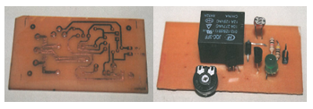
 | |||
| Figure 1 : PIC circuit |
 |
| Figure 2 : Relay circuit |
 |
| Figure 3 : LDR circuit |
The hardware circuit is design by using PCB board. To complete this
design, we need to follow the step above. The first one, we need to
aching the PCB board and then solder the circuit to make sure each line
will be connected with each other line.
Conclusion: -
For the conclusion after we design the circuit diagram in the program
software, we try on the PCB board to construct the circuit follow in the
software. The software help a lot on the design of circuit, follow the
PIC pin configuration and the port that we decide construct on the PCB
board.
No comments:
Post a Comment